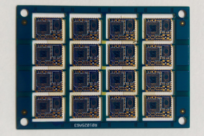
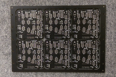
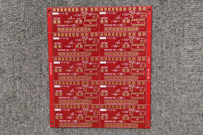
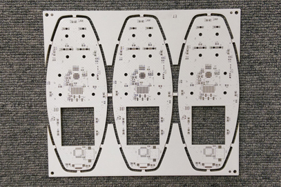
PCB
With the UL, ISO and QS certificated facilities in Taiwan, we can take 1 piece bare PCB quick turn job to high volume orders from you, from single side to 30 layers.
Nothing too small and no problem too big
To us, there is nothing called small order. We understand that quite often the speed and the accuracy of the PCB prototype is the key of how far you are ahead from others and how fast your products could be on the shelf in the market place. This is why we always take care of your prototype job the way just like we take care of the volume production.
In many cases, we work with customers to save their PCB tooling (NRE) cost if we know it could turn into production. We also provide our consultation to our customers if required to make the volume production built in most efficient way in term of time and money cost.
For your standard 2-10 Layers quick turn printed circuit board or prototype jobs, get to door price immediately from our on line PCB prototype price matrix table. The price you see is the price you are going to pay and shipping to your door is included. No extra charge, no hidden fee.
Process Capability
Laminate Material
| Base Material |
FR-4 TG135, TG150, TG170 |
| CEM1 |
| CEM3 |
| Rogers 3, 4 and 5 series |
| Arlon |
| Nelco 4000-13 |
| Alμminμm - 2L |
| Ceramic |
| Kapton |
| BT Material |
| Material Thickness |
3~240 mil (0.076mm ~ 6mm) |
| Min. board Thickness |
4mil. (0.1mm) - 2L |
| 14mils (0.4mm) - 4L |
| 24mils (0.6mm) - 6L |
| Max. / Min. Layer |
1 ~ 20L - Mass-Pro. |
| 22 ~ 26 L - Samples |
| Cu. Thickness |
0.3 ~ 10 Oz - Mass-Pro. |
Pattern Design
| Min. Line-width |
3 mils ( 0.076 mm ) -Mass-Production. |
| Min Spacing |
3mils (0.076mm) - Mass-Production |
| Image Distortion |
(+/- 20%) |
| Gold Thickness Range |
3~50μ" |
| Open / Short |
YES |
| Bow & Twist |
0.75% |
Solder mask
| Type Available |
Taiyo, Tamura, Onstatic |
| Green, Black, Blue, Red, White, Purple, Clear |
| Solder mask Registration tol. |
+/-3 mil |
| Min.Width S/M Bridge |
4 mil |
Peelable Mask
| PeelableMask Type |
Peters SD2955, SD2954,SD2952 |
| PeelableMask Thickness |
200μm |
Tolerance
| Routing |
+/- 0.005" |
| Feature to Hole |
+/- 4 mil |
| Hole to Hole |
+/-3 mil |
| Punching |
+/- 4 mil |
V-Cut
| V-grove Depth |
+/-10% |
| Min. Unit / Panel size |
100 mm |
| Min. Unit / Panel thick. |
3.2 mm |
Surface Treatment
| HASL Thickness Range |
80~1000 μm |
| Entek Thickness Range |
0.2~0.3 μm |
| Electroless Nickel Thickness |
100~200 μ" |
| Electroless Gold Thickness |
2~10μ" Max |
| Wire Bonding Gold Thickness |
5~10μ"Max |
| Lead Free HASL |
80~1000 μm |
| Immersion Silver |
6 ~12 μ" |
| Immersion Tin |
30~40 μ"(Include copper) |
| 15~20 μ"(Tin only) |
| Flux Thickness Range |
none |
| Carbon Print Thickness |
per resistor request |
| Carbon Print Res. |
per request |
Drilling
| Min. Final Hole Size |
6 mils ( 0.15 mm ) - Mechnical |
| Size |
4 mils ( 0.1 mm ) -Laser Drill |
| Hole size tol. |
PTH ±3 mil (+/-2mil for Press Fit ) |
| NPTH ±2 mil |
| Hole location tol. |
+/-3 mil |
| Layer to layer |
+/-3 mil |
| Registration tol. |
|
| Fiducial Mark Tolerance |
+/-20% |
| Board flatness Tolerance |
0.75% |
Special Requirement
| Epoxy In Holes |
|
| Vias In pad |
|
| Blind/Buried Vias |
|
QUICK TURN PRICE
Testing and tooling included
The dimensions below are the overall dimension per shipping lot.
Unit is in sq. inch. Currency: USD
Ex: Price of 495 sq. inches two layers board in 4 working days is $390.
Prices are based on standard spec, FR4 (Tg130), 1.6mm, up to 1oz start copper thickness, HASL finished, green solder mask and white silk screen, min. 4/4 mil trace width/space, min via 12 mil.
Lead time:
We start our working day (Monday to Friday) from 8:00am and finish at 20:00pm(Taiwan time). The lead time start from the first working 8:00am and boards will be shipped out before 20:00pm of the last working day. For example, if we receive your 2L job order with over all dimension 1480 Sq inches which requires 3 working days at 19:00 on Monday, we will ship it out no later than 20:00 that Thursday.
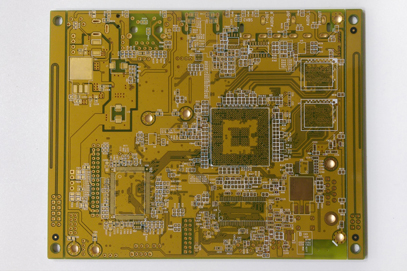
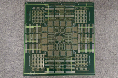
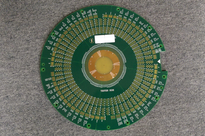
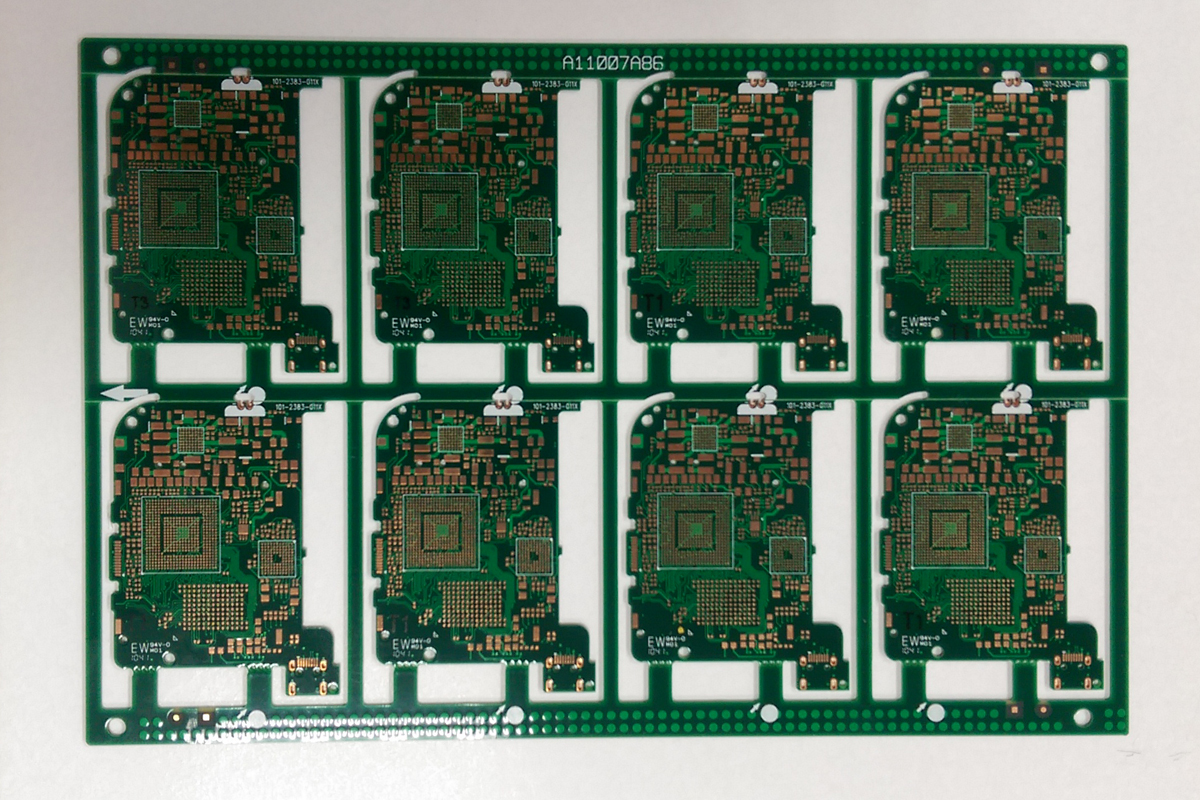
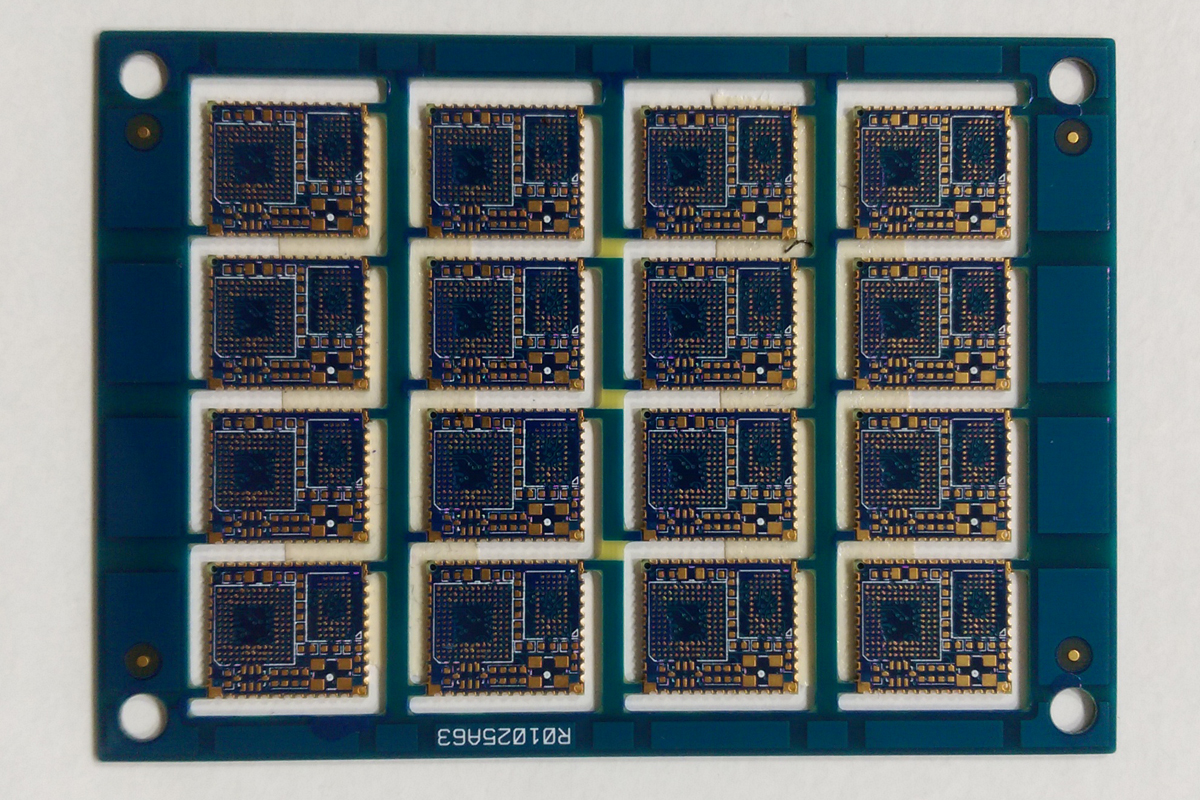
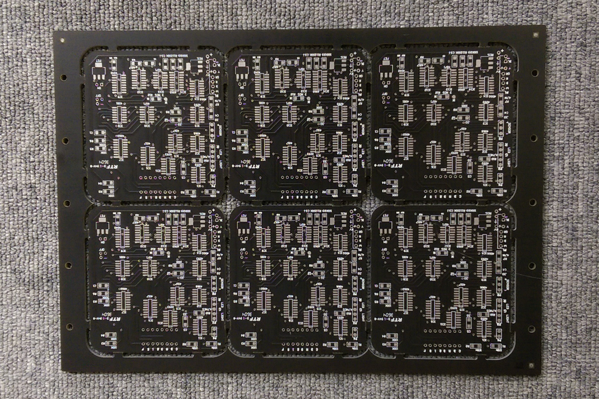
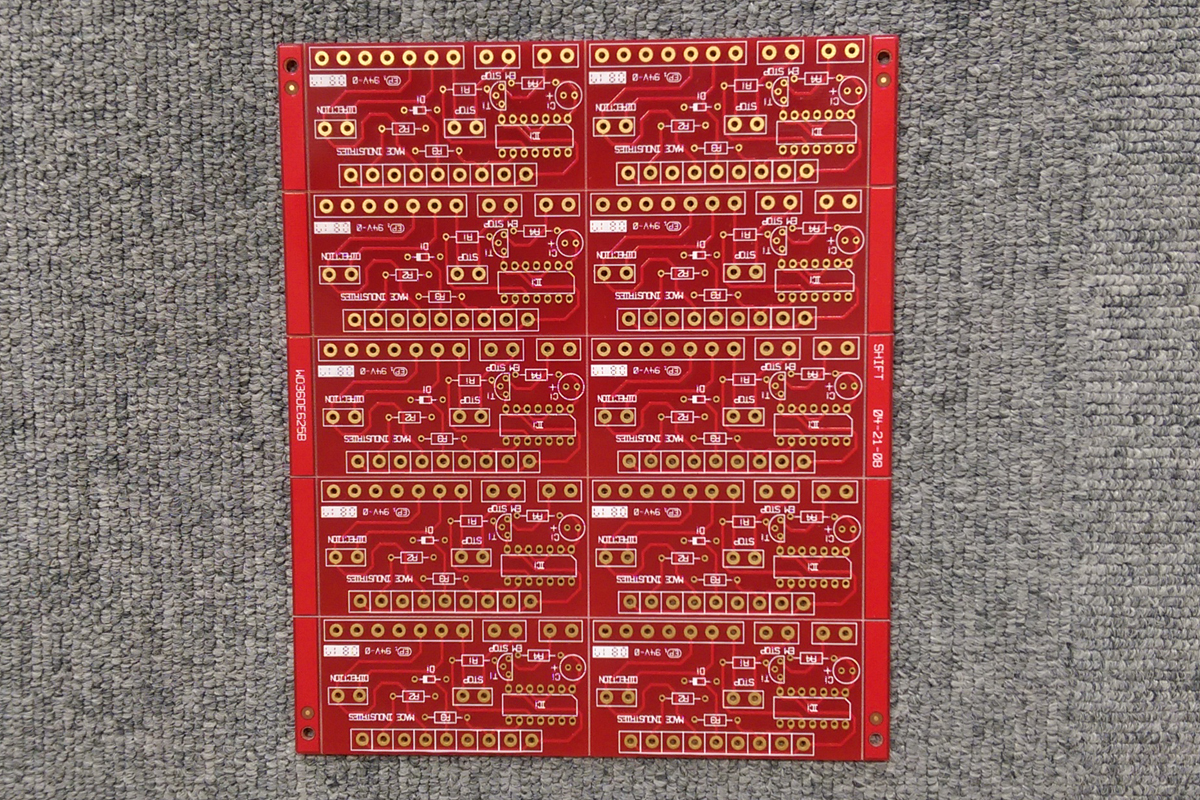
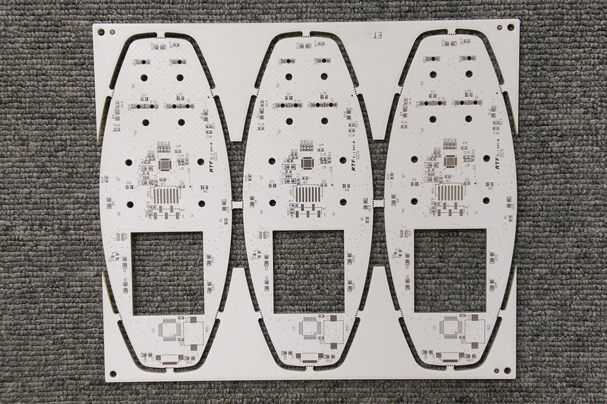
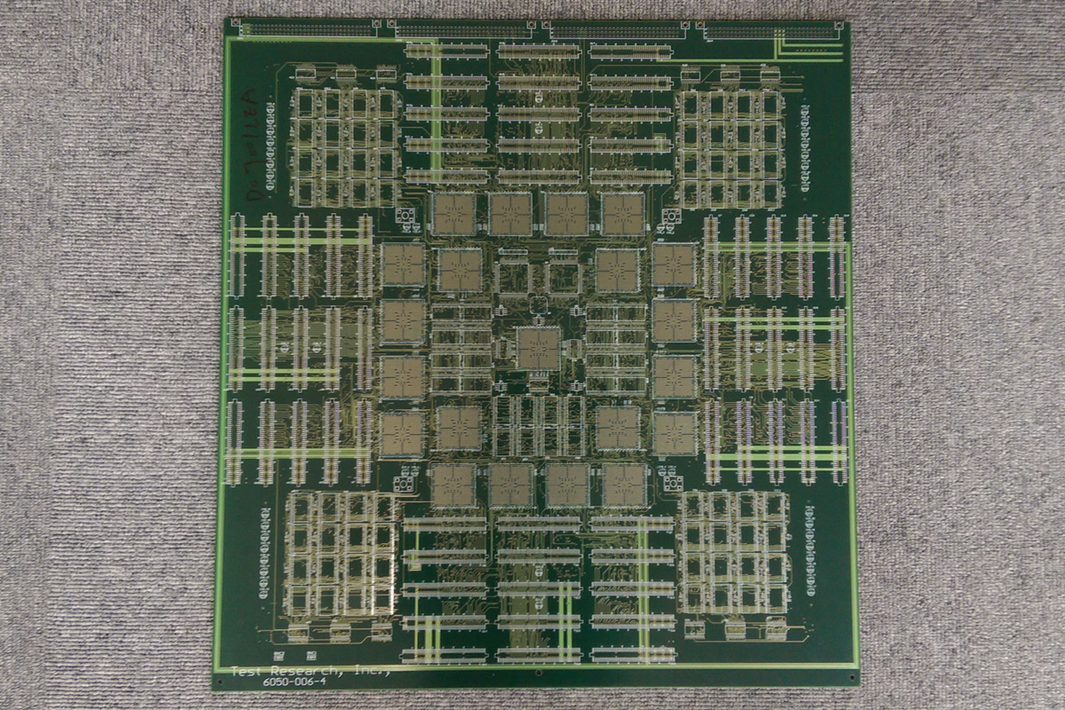
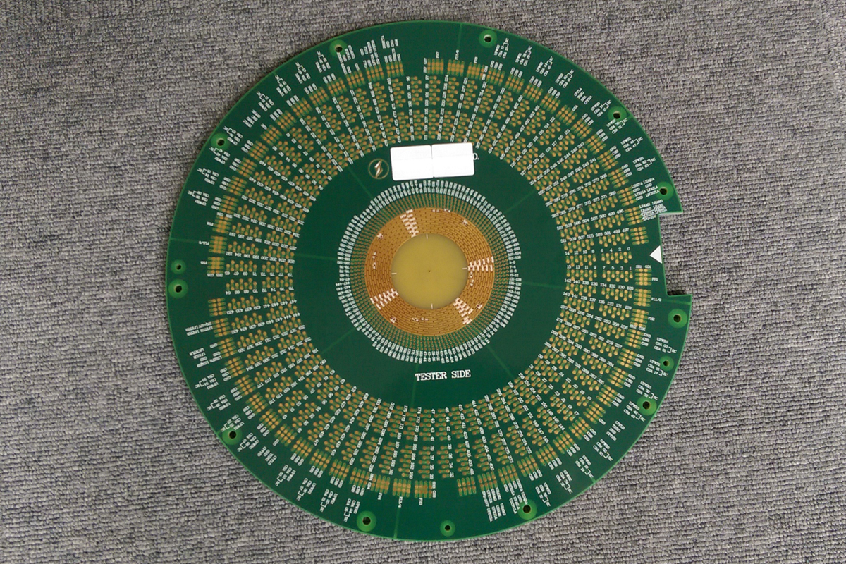
PRODUCTS
3 mils trace, 3 time lamination, 2 laser drill
Blind and burried via, edge plated,
Impendance control, epoxy filled via
Thick board with 6 mils via
