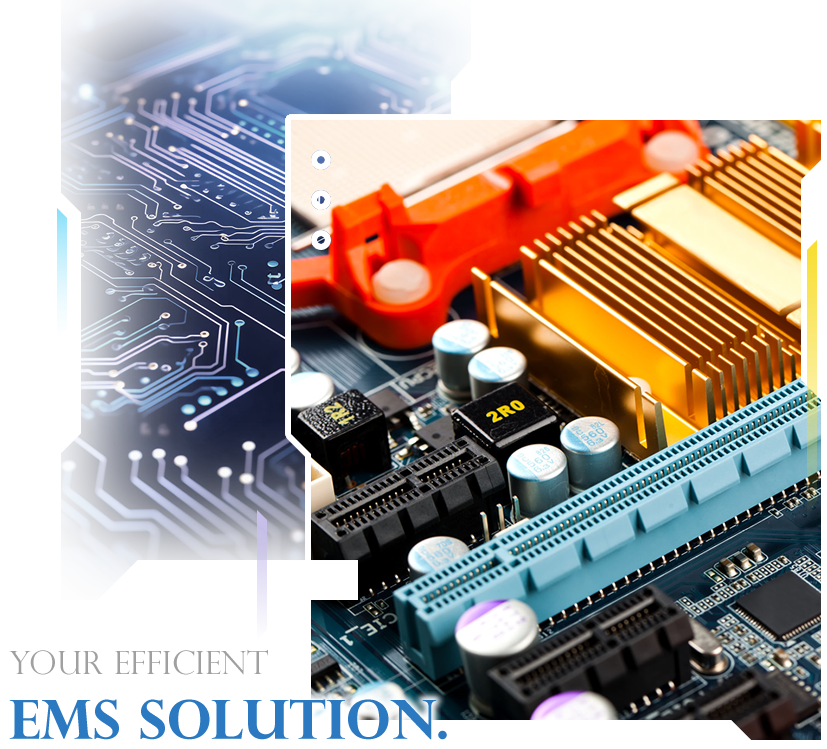
MISSION
使命與願景
追求卓越,提供完整的電子製造服務

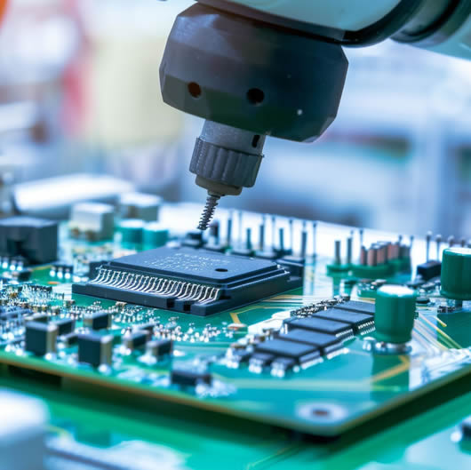
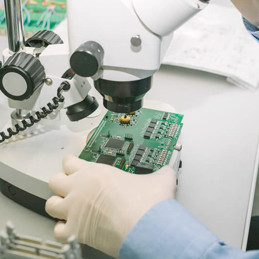
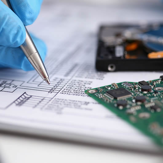
PRODUCT
全方位電子代工帶料夥伴
PCB / 整BOM備料 / 鐵塑機構件 / SMT / DIP / 組立 / 測試 / 物流運送
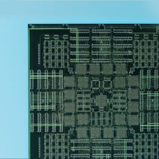
印刷電路板
PCB Fabrication
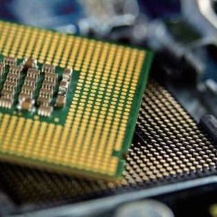
電子零件諮詢採購
Component Procurement
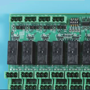
電子代工組裝
OEM PCB Assembly (SMT/DIP/Box build)
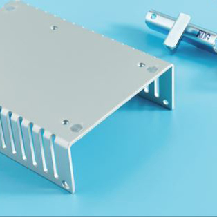
金屬及塑膠機構件
Metal and Plastic Parts
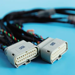
線材組裝
Cable Assembly